

Press text: Development of organic CMOS image sensor technology that achieves excellent color reproduction under all types of light sources

Panasonic Japan issued the following press text (google translated):
Development of organic CMOS image sensor technology that achieves excellent color reproduction under all types of light sources
Panasonic Holdings Co., Ltd. has developed excellent color reproduction technology that suppresses color mixture by thinning the photoelectric conversion layer using the high light absorption rate of the organic film and by using electrical pixel separation technology. In this technology, the organic thin film that performs photoelectric conversion and the circuit that stores and reads out electric charge are completely independent of each other. This unique layered structure reduces the sensitivity of each pixel in green, red, and blue in wavelength regions outside the target range. Since it can achieve spectral characteristics with low color mixing, accurate color reproduction is possible regardless of the type of light source.
[Overview] Conventional Bayer array silicon image sensors do not have sufficient color separation performance for green, red, and blue. Accurate color reproduction and color recognition and judgment were difficult.
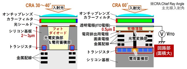
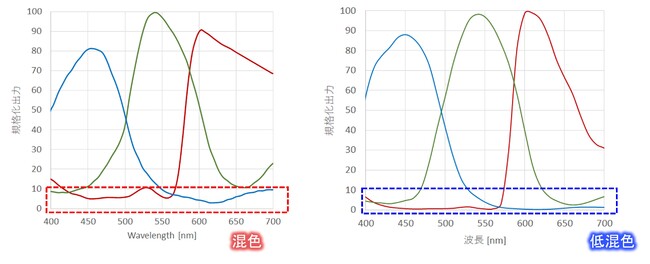
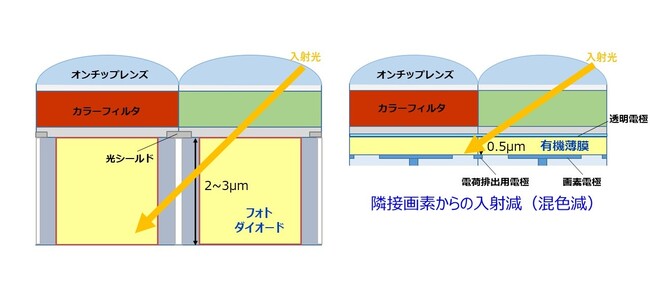
Hamamatsu organic CMOS image sensors have an organic thin-film photoelectric converter that converts light into an electrical signal, and an underlying circuit that stores and reads out signal charges. Figure 1). As a result, unlike conventional silicon image sensors, it is possible to provide photoelectric conversion characteristics that do not depend on the physical properties of silicon. Furthermore, we have achieved a thin film by using an organic film with a high light absorption rate ((1) thinning of the photoelectric conversion layer). By providing a charge discharge electrode at the pixel boundary, the signal charge due to the incident light at the pixel boundary is discharged and the signal charge from adjacent pixels is suppressed ((2) Electrical pixel isolation). . In addition, since the lower part of the organic thin film is covered with the pixel electrode for collecting the signal charge generated in the organic thin film and the above-mentioned electrode for discharging the electric charge, the incident light that could not be absorbed by the organic thin film is (3) Structure for suppressing light transmission). With the above technology, it is possible to suppress light and signal charges that enter from adjacent pixels. As a result, color mixture can be kept to a sufficiently low level, as shown in the spectral characteristics shown in Fig. 2, and accurate color reproduction is achieved regardless of the color (spectrum) of the light source (Fig. 3).
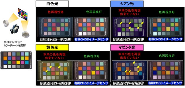
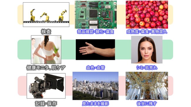
This technology enables accurate color reproduction and inspection even in environments where it is difficult for image sensors to reproduce the original colors, such as plant factories that use magenta light. In addition, since accurate color reproduction of substances with minute color changes such as living organisms can be expected, applications such as skin condition management, health monitoring, and fruit and vegetable inspection can be expected.
Furthermore, in combination with the high saturation characteristics and global shutter function (*1) of our organic CMOS image sensors, we will contribute to the construction of highly robust imaging systems that are resistant to changes in light source type, illuminance, and speed. .
(1) “Photoelectric conversion film thinning technology” that absorbs light up to 10 times
(2) “Electrical pixel separation technology” that discharges unnecessary charges at pixel boundaries
(3) Suppression of light passing through the photoelectric conversion section (1) Photoelectric
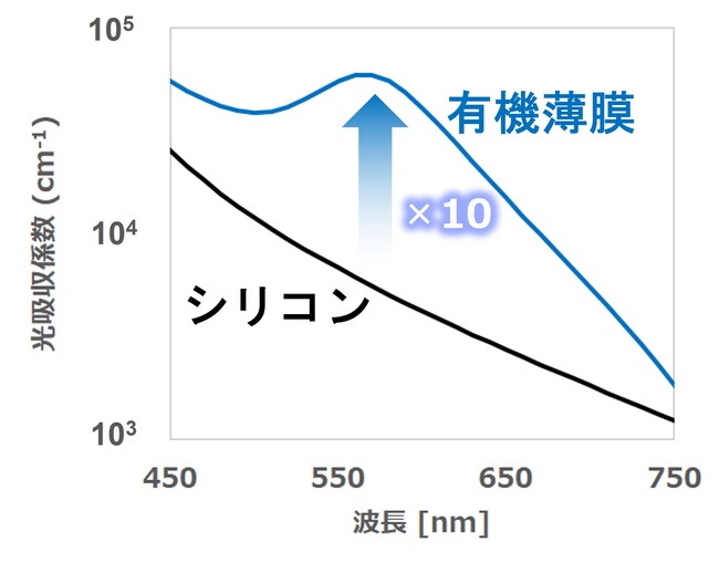
conversion layer thinning technology with up to 10 times higher light absorption The
newly developed organic thin film has a light absorption coefficient that is up to about 10 times higher than that of silicon (Fig. 4). ), which can shorten the distance required for light absorption. As a result, the organic film can be designed to be thinner than the silicon photodiode, and in principle, it is possible to reduce oblique incident light from adjacent pixels, which causes color mixture (Fig. 5).
(2) “Electrical pixel isolation technology” that discharges unnecessary charges
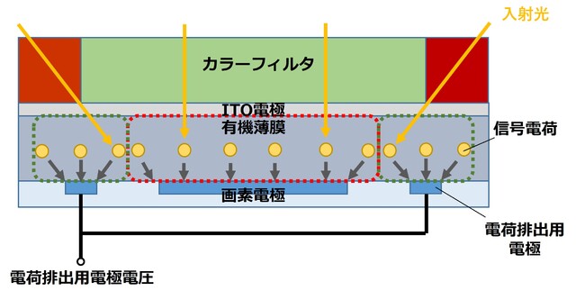
at pixel boundaries Charges generated at pixel boundaries include signal charges originating from adjacent pixels due to oblique incident light, which contributes to so-called color mixture and resolution degradation. becomes. In conventional silicon image sensors, a light-shielding layer is provided at the boundary between pixels to prevent oblique incident light. There were inadequate aspects such as going around and invading.
Therefore, by arranging a charge discharge electrode at the pixel boundary, we have developed a structure that discharges the signal charge due to the incident light at the pixel boundary and suppresses the intrusion of the signal charge from the adjacent pixels. By providing a charge discharge electrode, the charge generated at the pixel boundary can be discharged, thereby suppressing the image quality deterioration described above (Fig. 6).
(3) “Light transmission suppression structure” that suppresses the transmission of
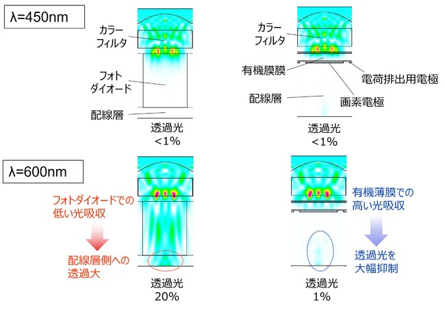
light through the photoelectric conversion section. converted to signal charge. However, some of the light is not photoelectrically converted and passes through, contributing to color mixture. In particular, red light, which has a longer wavelength and lower energy than blue light, is easier to pass through and has a greater effect.
Conventional silicon image sensors transmit about 20% of light with a wavelength of 600 nm, but the developed organic CMOS image sensor has a significantly reduced transmission of about 1% (Fig. 7). The lower part of the organic thin film is covered with the pixel electrode for collecting the signal charge and the aforementioned charge discharging electrode. Therefore, incident light that cannot be completely absorbed by the organic thin film is absorbed or reflected by the electrode and is absorbed by passing through the organic thin film again. In addition, since the space between the pixel electrode and the charge discharge electrode is very small, the structure is such that light does not easily pass through the lower part of the organic film.
Going forward, we plan to propose these organic CMOS image sensor technologies for a wide range of applications, including commercial broadcast cameras, security cameras, industrial inspection cameras, and automotive cameras. We will contribute to the construction of imaging systems.
*1 [Press release] Development of 8K high-resolution, high-performance global shutter imaging technology using CMOS image sensor using organic thin film
https://news.panasonic.com/jp/press/jn180214-1
array One of the arrays of color filters mounted on each pixel to obtain color information, which is repeatedly arranged in units of 4 RGGB pixels. Since each pixel has only one of R, G, B color information, other color information is interpolated from surrounding pixels.
[2] The signal of a pixel with mixed colors is mixed with adjacent pixels. In a Bayer array image sensor, since adjacent pixels have different colors, color signals are mixed, resulting in a state in which accurate colors cannot be reproduced.
[3] Color reproducibility
How well the captured image can actually reproduce the color of the subject. It is affected by the spectral characteristics of the image sensor, the spectrum of the light source, and the reflection spectrum of the subject. [Contact] Panasonic Holdings Co., Ltd.
Public Relations Email: crdpress@ml.jp.panasonic.com